Case Study: “Quark” Hardware Interface Prototype
Project Overview The “Quark” project was a developmental prototype focused on creating a compact, knob-driven hardware interface. This project served as an initial proof-of-concept for transitioning into Surface Mount Device (SMD) Printed Circuit Board design, involving end-to-end execution from CAD to final assembly and testing.
Hardware Design & Assembly The mechanical footprint of the device was designed in CAD, and the board outline was exported as a DXF to define the physical constraints in EasyEDA. The board design required careful component placement on both sides of the PCB and manual trace routing, guided closely by manufacturer datasheets.
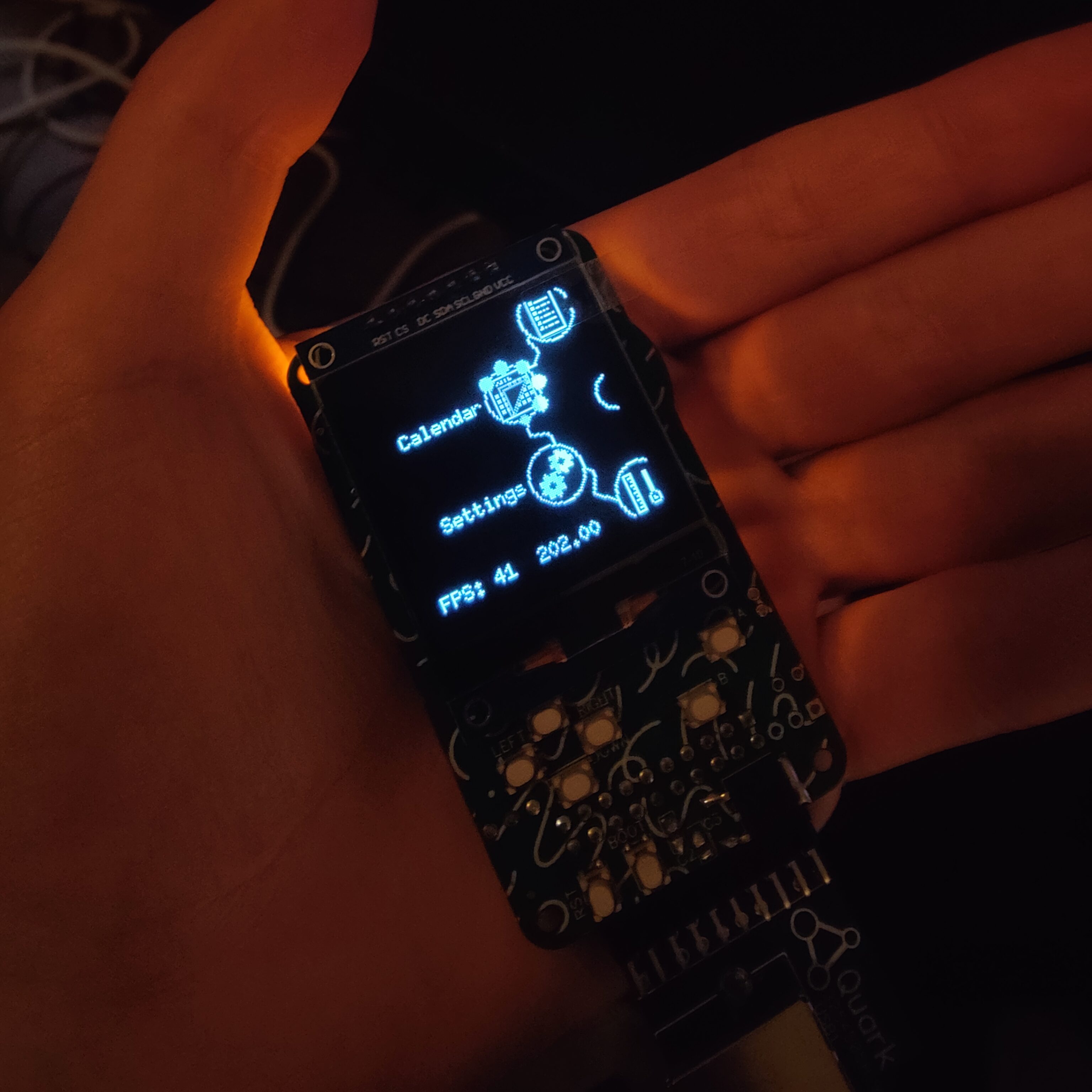
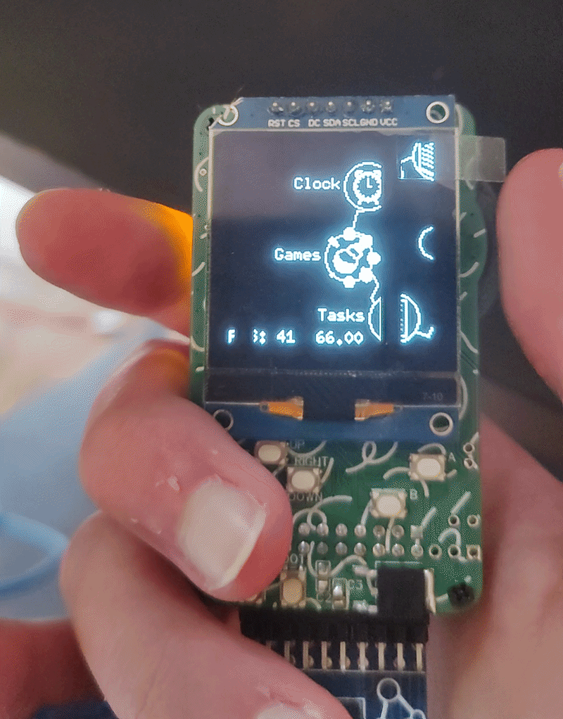
Once the Gerber, BOM, and Pick-and-Place files were generated, the boards were sent to JLCPCB for fabrication and partial assembly. The factory assembly successfully handled the core SMD components, demonstrating the viability of low-cost PCBA for rapid prototyping. Upon receiving the boards, I completed the final manual soldering for the through-hole components, including the display and the main interface knob.
Testing & Iterative Learning Initial bring-up was successful. The device ran custom firmware and rendered accurately to the attached display, validating the core schematic and the PCBA manufacturing workflow.
During extended testing, a specific hardware vulnerability was identified: the magnetic field generated by the physical knob induced interference, causing instability on the microcontroller’s SPI bus. While this interference prevented the current revision from functioning as a long-term standalone device, identifying this edge case provided a clear engineering constraint for future designs.
Ultimately, the project succeeded in its primary goal of validating a rapid SMD prototyping pipeline, while reinforcing the critical importance of electromagnetic shielding, trace routing, and component isolation when designing hardware with integrated magnetic mechanics.